Project Description
In this project I describe the construction of a Trapdoor memory extension for the AMIGA A500 with 1.8 or 2 MB of RAM. In a A500 Rev 6A or newer, it can be configured to extend the ChipRAM to 1MB. It uses a GARY-adapter that can also be used independently as a replacement for a large range of GARY adapters used in other trapdoor memory extension.
Requirements
- [Required] To program the GALs with the JEDEC files provided, you need a GAL programmer. I use the TL866 available from E-Bay for around 50€. It works well and can be used for many other projects too.
- [Required] Soldering equipment and the usual electronics tools.
- [Optional] If you want to adapt and recompile the source code you need something to do that. WinCUPL is good enough and available for free from Microchip.
- [Optional] To change the PCB files use the incredible KiCad.
Files
- Schematics of the Trapdoor PCB (PDF)
- Schematics of the Gary Adapter T3 version (PDF)
- Schematics of the Gary Adapter T4 version (PDF)
- Full Package on GitHub
Theory of Operation
1. A normal Trapdoor extension
It helps to check the schematics of an AMIGA and that of an ordinary trapdoor extension as for example in the excellent schematic of an A500 Rev 6A available here. In the AMIGA, the internal DRAM and the DRAM on a trapdoor extension is manged by the DRAM controller built into AGNUS. It is activated by the signal /RAMEN generated by GARY based on the adress on the bus. The /RAMEN signal is active (ie. low) whenever the CPU tries to access an address in the ChipMem-Range (this is 0x000000-0x1FFFFF) or in the RangerMem address range (0xC00000-0xC7FFFF). When this happens, AGNUS multiplexes the adresses A18-A1 to the address bus DA8:0 of the DRAMs. The procedure is the following:
-
- First, one half of the adresses A18-A1 is assigned to DA8:0
- If the access is to ChipMem, then AGNUS asserts /RAS0, otherwise, the access is to RangerMem and AGNUS asserts /RAS1. The distinction is made based on the status of A19.
- The remaining adresses are assigned to DA8:0.
- AGNUS asserts /CASL and/or /CASU depending on whether the CPU wants to do a bytewise or wordwise access.
To refresh the DRAM, AGNUS does a RAS-only access with incremented addresses on DA8:0. The exact procedure is the following:
-
- AGNUS generates an incrementing sequence of row adresses and assigns it to DA8:0.
- Both, /RAS0 and /RAS1 get asserted.
A standard 512k Trapdoor extension connects to the DRAM adresses DA8:0, to /RAS0, /RAS1, /CASU, and /CASL. Hence it can decode 2^18 = 256k adresses of 2 Byte words. This is exactly what is needed to cover the RangerMem address space.
2. What we need for more memory
From the above description, we see that to introduce more memory into the system, we have to do the following things:
-
- Find a memory range that is scanned by the kickstart and made available if there is memory there.
- Trick GARY into asserting /RAMEN, if the CPU accesses this range.
- Make sure that there is memory available at these adresses.
- Decode the CPU adresses to the memory extension.
- Make sure that the refresh works for our memory extension.
The answer to the first question is easy. Upon (cold) reboot, the kickstart detects whether there is memory available in the address range C00000-DBFFFF and if this is the case, the memory there is added to the system on boot. This range covers 1792k or roughly 1.8MB of memory adresses. It is called the Ranger Memory Area. (But I don’t know why).
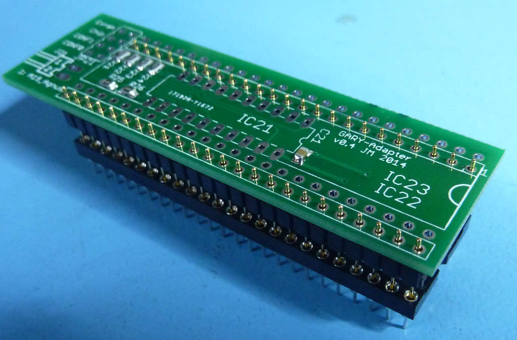
The Gary adapter (T3 version)
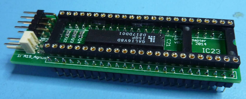
Answering questions 2-4 is the task of the GARY adapter. This is mainly a little PCB connecting to the GARY socket, evaluate the CPU adress lines and fake a few signals to GARY. The essential device is a GAL, ie. programmable logic to allow us to do the functions required in an efficient way. It does the following:
-
- Monitor the CPU-Adresses A23:17 to see whether the CPU accesses the ranger memory. If this is the case, then we show GARY a address in the range C00000-C7FFFF so that it asserts /RAMEN. In the file gal-gary/GARY2.PLD this corresponds to the lines:
addr_08 = (!a23 & !a22 & !a21 & !a20 & a19);
addr_C0 = ( a23 & a22 & !a21 & !a20 & !a19);
addr_C8 = ( a23 & a22 & !a21 & !a20 & a19);
addr_D0 = ( a23 & a22 & !a21 & a20 & !a19);
addr_D8 = ( a23 & a22 & !a21 & a20 & a19 & !a18);
!a19_out =   !a19
           # addr_C8 & !NCONF0 & !NEXRAM & NCHIPRAM_SW
           # addr_C8 & !NCONF1 & !NEXRAM
           # addr_D8 & !NCONF0 & !NCONF1 & !NEXRAM & NCHIPRAM_SW;
!a20_out =   !a20
           # addr_D0 & !NCONF1 & NCHIPRAM_SW & !NEXRAM
           # addr_D0 & !NCONF1 & !NCONF0 & !NEXRAM
           # addr_D8 & !NCONF0 & !NCONF1 & !NEXRAM & NCHIPRAM_SW
The fist couple of lines do the address decoding by comparing the address lines. Fixing five address lines A23:19 gives us blocks of 512k memory, but the D8 block is only 256k of size, because it ends on DBFFFF. Note that we are also decoding accesses to the memory area 080000-0FFFFF. This is used later for the Chipram feature. The next lines do the address faking for GARY. We condition this with the setting of four input signals, NCONF0, NCONF1, NEXRAM, and NCHIPRAM_SW, all of them are active low. NEXRAM selects whether the Ranger Memory should be available. NCHIPRAM_SW selects whether we use one of the four available memory banks as a ChipRam extension, which will be visible for the CPU at the address range 080000-0FFFFF. NCONF0 and NCONF1 determine how many banks should be made available in total. If both of them are zero, all four banks are used.
- Decode the true address from the CPU to four memory banks:
bank0 = (addr_C0 & NCHIPRAM_SW) # (addr_08 & !NCHIPRAM_SW) # (!NBLIT & !NCHIPRAM_SW);
bank1 = (addr_C8 & NCHIPRAM_SW) # (addr_C0 & !NCHIPRAM_SW & NBLIT);
bank2 = (addr_D0 & NCHIPRAM_SW) # (addr_C8 & !NCHIPRAM_SW & NBLIT);
bank3 = (addr_D8 & NCHIPRAM_SW) # (addr_D0 & !NCHIPRAM_SW & NBLIT);
Here, we generate the bank signals. Bank 0 gets activated if access is to C00000-C7FFFF and chipram is not activated or if the access is to 080000-0FFFFF if chipram is activated. It is also activated, if the Chipset is accessing the Chipmem. This is the case if NBLIT is low. In this case the CPU address is meanigless, so we can not use it. The other banks are only activated by CPU acesses, so we have to test whether NBLIT is high in this case.
- Generate select signals from the bank selection:
sel0.d = bank1 # bank3;
sel1.d = bank2 # bank3;
These signal binary encode the bank number that has to be activated. They are attached to the connection between the GARY adapter and the trapdoor card. They are latched by a rising edge of the CCK signal, because the NBLIT signal get deasserted, before the Ram-cycle is complete. This would interfere with the Chipset accessing our extended ChipRam.
- We have to do one other thing. In a normal AMIGA, the highest address pin connected to AGNUS is A23 (it is th A19 Pin as seen by Agnus). It is zero, if the CPU accesses the usual 512k Chipmem in the range 000000-07FFFF, it is one if the access is to C00000-C7FFFF. This is the way how AGNUS decides whether the access is to the built-in memory and /RAS0 has to be activated, or to the trapdoor slot and /RAS1 has to be activated. Our extension will reside in the trapdoor slot, but it will also need to serve the address range 080000-0FFFFF. In this range A23 is low, and AGNUS would activate the internal memory. To enable chipram extensions the AMIGA Mainbords have a jumper to change this behaviour and connect A19 from the CPU to A19 on AGNUS. This does the right thing for a ChipRam extension. This Jumper is JP2 on a REV5, Rev6A or REV8A AMIGA 500 board. We do the switch in the GAL, depending on whether we want the ChipRam extension or not. Not that we have to or with A23 to also activate the external trapdoor slot in the whole Ranger Mem address space.
a19_agnus = a23 # (a19 & !NCHIPRAM_SW);
- Monitor the CPU-Adresses A23:17 to see whether the CPU accesses the ranger memory. If this is the case, then we show GARY a address in the range C00000-C7FFFF so that it asserts /RAMEN. In the file gal-gary/GARY2.PLD this corresponds to the lines:
This is the version of the GARY adapter that computes the bank select singals. They are processed further on the memory board to generate an address line for the DRAM chip. There is a different version of the GARY adapter (called the T4 version) that generates the address line. This will be described after we describe the memory board.
The memory board
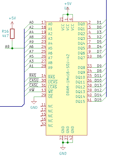
The memory board is basically a connection between the RAM chips. Here we chose one DRAM with 1M x 16. This means that the chip has 16 data lines, and 2^20 = 1M different addresses. This fits the 16 Bit wide data bus of the AMIGA. This gives a total of 2MBytes of memory. DRAMs load the current address in a two step process to save address pins, so our RAMS have only 10 address pins A0:9. First, the memory controller assigns half of the adresses (the row address) on the address pins and determines via RW whether this is a read or write access. Then it pulls RAS low, asserts the second half of the address (the column address) to the address pins and pulls CAS low.
 After the access time of the DRAMS, the data of a read appears at the data pins, or the data is written to the internal memory. In both cases the cycle ends, when RAS and CAS are released to their idle high state.
In the Amiga, Agnus usually does all of this and also provides the adresses A0:8. Nine address pins give 256k addresses, for the usual 512kB of memory in the tradoor slot. To extend this, we have to provide the new address bit A9. We generate this form the bank select signals SEL0:1. SEL0 becomes the row address and SEL1 the column address. To this end, we set A9 to SEL0 if RAS and is high, and to SEL1 if it is low. There is a slight complication, as the DRAM have a specified time of how long the address must be held constant after the transition of RAS to low. This is why we do not use RAS directly as multiplexing singnal, but delay it by sending it through three invertes external to the GAL. The resulting equations become:
RAS_out = !RAS1_IN & RAS0_IN;
A9 = SEL1 & NRAS_delay # SEL0 & !NRAS_delay;
Here RAS_out goes through the invertes and the result is inverted NRAS_delay. The RAS_out equation only becomes high, when RAS0_IN is high and RAS1_IN is low. This indicates a true memory access to the trapdoor slot.
We have to accomodate for one other fact. DRAMs tend to forget their contents and need to be refreshed constantly. In the Amiga this is done using RAS-only refresh. Here, Agnus asserts a increasing sequence of row addresses and pulls both RAS0 and RAS1 low and keeps the CAS lines high. This refreshes the corresponding row in both, the internal and trapdoor memory chips. The problem is, that Agnus does not generate enough row adresses, because it only serves address lines A0:8. Fortunately, the more modern (as compared to 256kx1 types) DRAMs we use here, support a refresh called CAS-before-RAS refresh. In this mode, the chip internally generates the row address and we only have to trigger the refresh. It works by first assering CAS and after that asserting RAS. We still use Agnus to time this refresh. A refresh cycle can be distinguished from a normal memory cycle, since then both RAS lines go low. Consider the following code:
REFRESH = !RAS0_IN & !RAS1_IN;
!CASL = !CASL_IN # !RAS0_IN & !RAS1_IN;
!CASU = !CASU_IN # !RAS0_IN & !RAS1_IN;
!RAS = !RAS1_IN & RAS0_IN # REFRESH_delay;
The first line detects the refresh cycle. It outputs a signal to two invertes in a row (again external to the GAL). The resulting signal is called REFRESH_delay. The two CAS lines get asserted if either Agnus asserts these lines or a refresh is going on. The RAS line gets asserted by a memory access to the trap door slot, when RAS1 is low and RAS0 is high, or as part of the CAS-before-RAS refresh if the delayed REFRESH signal goes low. The delay is necessary to meet the requirements of the timing for the CAS-before-RAS refresh.
The alternative GARY adapter (T4)
The idea described here was shared with me by Paradroid at the A1K forum. The previously described solution leads to a pair of PCBs which need to share two signals, SEL0 and SEL1. Hence we have to run two cables from the GARY adapter to te trapdoor PCB. However, from this we generate only one signal for the DRAM, namely A9. This in itself would not be very interesting, but notice, that the A500 PCB includes one exclusive connection from GARY to the trapdoor slot, the EXRAM line. If we were able to generate the A9 signal on the GARY adapter, we could use this line to send it to the DRAM. A9 is multiplexing the SEL0 and SEL1 signals depending on whether we are sending the row address or the column address. The AMIGA uses the color clock (actually a phase shifted version of it, called CCKQ) to change from RAS to CAS. RAS goes low on the rising edge of CCKQ. Thus we write
bank0 = addr_C0 & NBLIT;
bank1 = addr_C8 & NBLIT;
bank2 = addr_D0 & NBLIT;
bank3 = (addr_D8 & NCHIPRAM_SW) # (addr_08 & !NCHIPRAM_SW) # (!NBLIT & !NCHIPRAM_SW);

sel1 = bank0 & CCK # bank1 & CCK # sel1 & CCK # sel1 & CCKQ;

da9_out = bank0 & !CCKQ # bank2 & !CCKQ # sel1 & CCKQ;
da9_out the the A9 signal we generate. The first two terms encode SEL0, the second switches to SEL1 when CCKQ is high. Note that we have to hold SEL1 fixed as long as CCKQ is high, this is the role of the last term in the SEL1 equation.
The problem with this setup is, that AGNUS does not pull RAS low exactly at the rising edge of CCKQ and also that we have to meet the hold time of the address after RAS going low. Thus we have to delay the DA9_out signal further by feeding it to an inverter chain on the trapdoor board. The GAL there does this with the equations
A9_to_delay = A9_in;
A9_out = A9_from_delay;
As we are using three inverters in series, the actual A9 signal is inverted, but this does not matter since it only permutes the order of the banks. The remaining logic stays the same.
Building it!
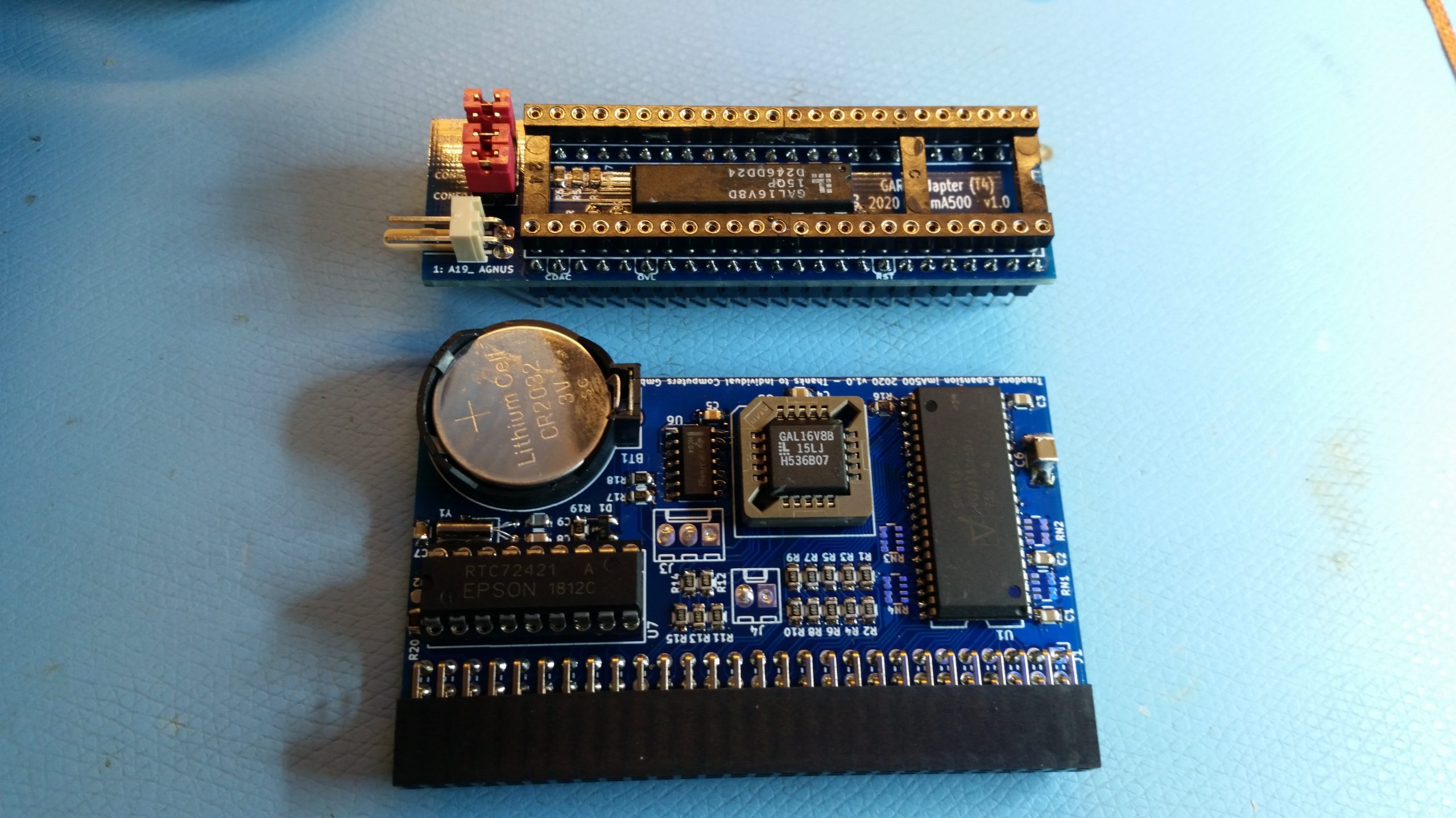
Here I describe building the T3 version. The T4 version is similar and differs only slightly in the instalation. The PCBs can be ordered from several PCB manufacturers using the kicad files provided. Note that I chose the footprints for easy hand soldering, so they are most likely not suitable for automated manufacturing.
The Gary adapter (T3 version)
| C1 | 100nF 0805 |
| IC1 | Socket 48 Pin DIP |
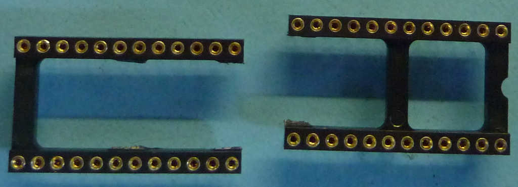
| IC2 | 2×24-Pin IC Adapter Pins |
| IC3 | GAL 16V8 DIP2 |
| J1 | PSK3 with corresponding connector |
| J2 | 2×3 Pin Header Straight 2.54mm and three Jumpers |
| R1,2,3 | 68R 0805 |
| R3,4,5 | 4k7 0805 |
- Program the GAL with the file GARY-T3.jed from the directory gal-gary in the github repository. This is important, the GAL can not be programmed in circuit.
- Solder the SMD parts to the PCB.
- Then use the socket to align the IC adapter PINs and solder them.
 Note that the PCB here is different, but the idea is the same. Also, the IC adapter Pins go into the same location.
 - Some sockets will not allow for mounting the GAL inbetween. Maybe you have to cut some plastic away to make room for this. To illustrate, here is an example where I use two sockets with 24 pins
- Solder the GAL, the socke and finally the connectors.
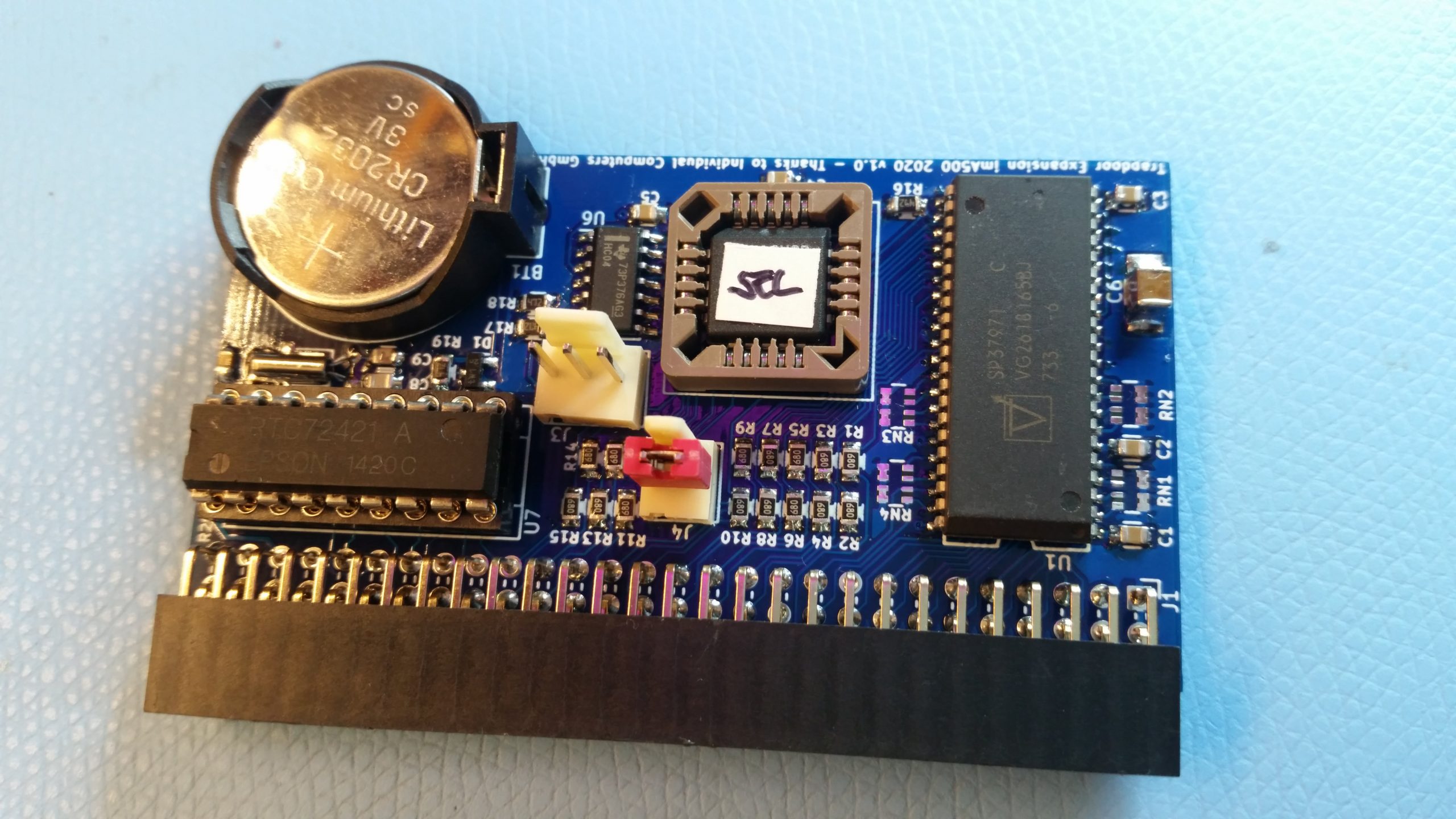
The Trapdoor PCB
The trapdoor PCB fits both versions of the GARY adapter, the only difference is the program for the GAL. These parts are still easy to obtain as they are quite generic parts. For example you can order ATF16V8 from reichelt.de. The trapdoor conector is a standard angled 2x28Pin socket for 2.54mm pins also available from there along with the other parts. For the clock chip you can use the original MSM6242 from OKI or a pin-compatible EPSON RTC72421. this one even includes the crystal, which then can be omitted from the PCB.
| Identifier | Case and Value | Number |
| C1-5 | 100nF SMD 0805 | 5 |
| C6 | 10µ SMD 1206 or 1210 | 1 |
| J1 | Pin Socket Angled 2×28 Pitch2.54mm | 1 |
| J3 | PSK 3, 3×2.54mm_Straight, omit on T4 | 1 |
| J4 | PSK 2, 2×2.54mm Straight, omit on T4 | 1 |
| R1-15 | 68R SMD 0805 | 15 |
| R16-20 | 4k7 SMD 0805 | 5 |
| RN1-4 | omit | 0 |
| U1 | DRAM 1Mx16 in SOJ-42 | 1 |
| U5 | PLCC-20 SMD-Socket, GAL 16V8 | 1 |
| U6 | 74HC04 SOIC-14 | 1 |
| BT1 | Batter holder CR2032 with battery (optional for RTC) | 1 |
| C7 | 1µ SMD 0805 (optional for RTC) | 1 |
| C8-9 | 22p SMD 0805 (optional for RTC) | 2 |
| D1 | BAT54C, SOT-23 (optional for RTC) | 1 |
| U7 | Socket DIP-18 and MSM6242 or RTC72421 (optional for RTC) | 1 |
| Y1 | Crystal 32.768kHz (optional for RTC, not needed for RTC72421) | 1 |
The only part that is a bit tricky to get is the DRAM. There are a few suitable part numbers. Make sure to get a 5V part, a similar architecture is also in 3.3V which will not work. I found a couple of offers on ebay but would recommed staying clear of those. I rather desolder these chips from a PS/2 memory module.
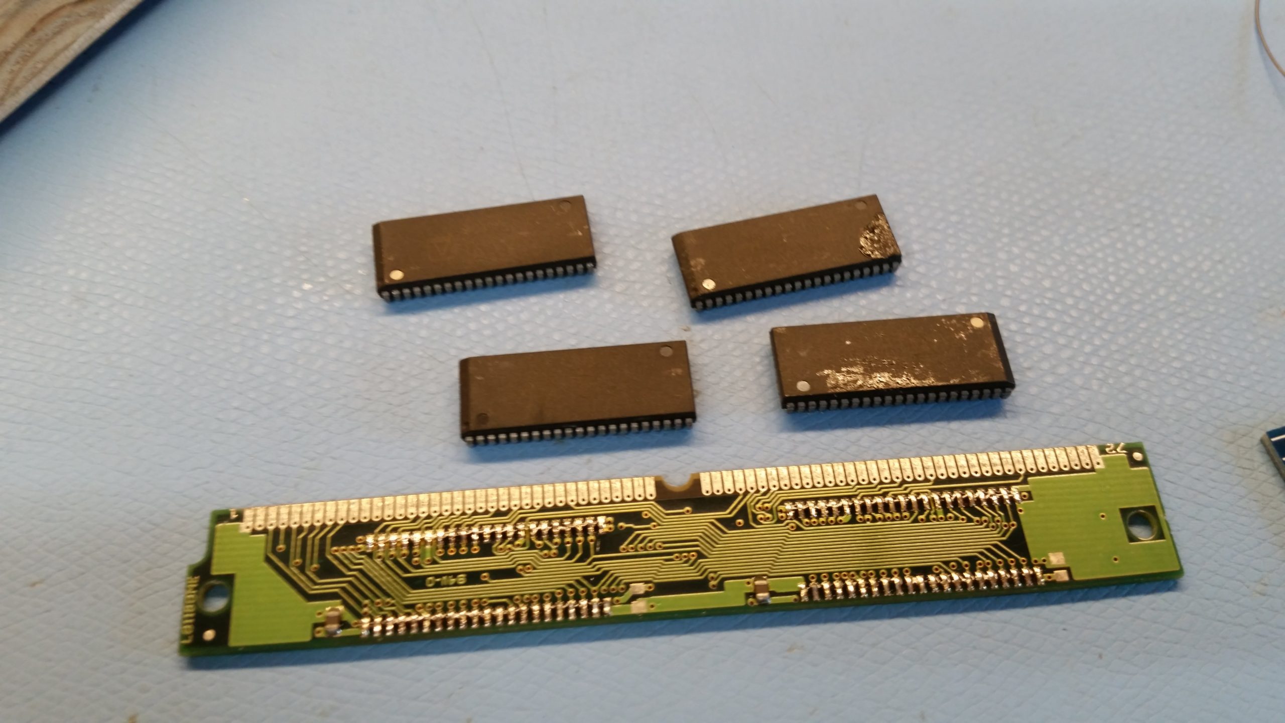 Here I desoldered a 8MB module with four chips (two on both sides). There are also 4MB modules with two chips.
Program the GAL with the file corresponding to the GARY adapter chosen. Use CBR5SEL.jed for a T3 adapter and CBR5EX.jed for a T4 adapter. Using the wrong file will not work, but will not damage your AMIGA.
Soldering is not difficult. I suggest to start with the SMD capacitors (except C6, it will block easy access to some pins of the DRAM), the resistors, the diode and U6. Then solder the DRAM and C6 after that. If you want, you can use a socket for the GAL, if you want to experiment with it. To solder it, break out its bottom, so that you can access the pins with your soldering iron: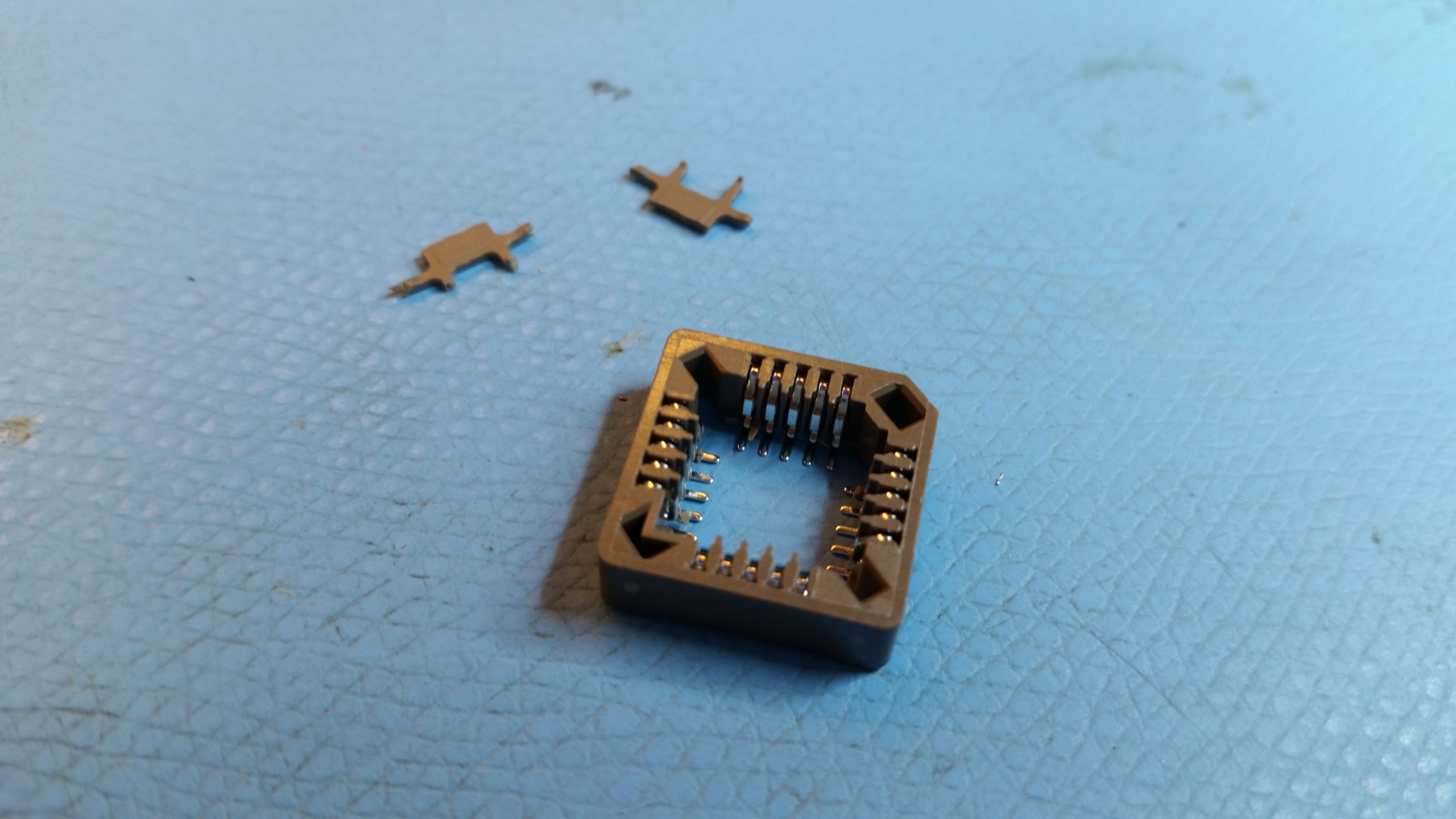 Otherwise solder the GAL on the pads. The remaing parts can be soldered in any order. Make a thorough visual inspection of your soldering, in particular check for good connections of the GAL and DRAM pins. In principle you are ready for a test.
Installation
If you are confident that you don’t have any soldering mistakes, you can install the GARY adapter and the Trapdoor PCB into your AMIGA. On the T3 GARY connect J1 pins 1 and 2 to the Trapdoor board J3 pins 2 and 3 (in no particular order. The T4 GARY adapter does not need any further connection to the trapdoor board. For now ignore Pin 3 of J1 on the T3 GARY adapter or Pin 1 on J2 of the T4 GARY adapter. On the GARY adapter set jumpers CONF0 and CONF1, on a T4 also the EXRAM jumper. With a T3 GARY adapter the EXRAM jumper is J4 on the trapdoor board and also needs to be closed. Do not close this on a T4 board. Boot your AMIGA with a Workbench disk. The program MergeMem in the System folder should tell you that there is SlowMem avaiable from the adress C00000 to DBFFFF. If not, check your PCBs.
If you have a Rev 6A board with an AGNUS 8372, then you can use one bank of the trapdoor memory as a ChipRAM extension. This will not work with an 8371. This requires a connection from the GARY adapter to the middle pin of jumper J2 on the AMIGA mainboard (near the Kickstart chip). On a T3 GARY adapter, the signal needed is on Pin 3 of J1, on a T4 it is on Pin 1 of J2.
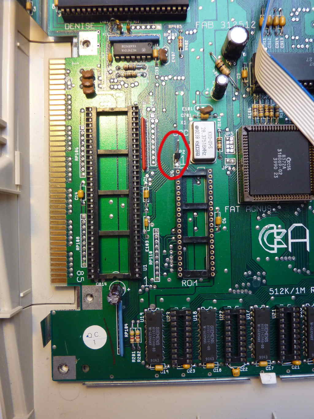 In an original AMIGA There is a connection beween Pins 1 and 2 of that jumper. It has to be cut and Pin 2 has to be connected to the signal generated on the GARY adapter. Cutting this connection is not trivial, make sure that you cut towards the chrystal so that you do not damage the fine PCB traces on the other side in case you slip. In my Amiga, the middle pin had a hole, so that I could solder a pin for a non-permanent connection. If you now close the CHIP jumper on the GARY adapter, your AMIGA will report 1.5 MB of SlowRAM, but 1MB of ChipRAM.